![[figure 1]](fig1.gif)
by Shawn Hunt
This article appeared in the July 1996 issue of Recording Magazine.
With the digital revolution in audio, it might seem like the good old days of building project circuits is gone. Sort of like the auto industry. Lots of old cars were perfect for the Sunday mechanic, but how do you give a tune up to that computer under the hood? Turns out, however, that digital projects are not more complicated than for analog, just different. The sample rate converter built here is a straightforward project, and should be no problem for the expert or beginner. All that is needed is a little patience, and a steady soldering hand.
When the digital revolution came upon us, first with the effects processors, then with digital tape and hard disk recording, the inputs and outputs were still analog. This was mainly because most other equipment was still analog, but also because it is easier to have analog connections. With analog, the only things to worry about are impedances and levels. Levels can usually be controlled, so as long as output impedances were relatively low, and input impedances were relatively high, just about any piece of equipment could be connected to another. Making things even easier, there are only two types connections used, balanced and unbalanced, and although not optimal, even these can be connected together. There are more variations in the digital domain, and they are usually incompatible.
In a piece of digital equipment, three signals are typically used internally when transmitting data from one chip to another: The digital bits making up the data signal, a bit clock, and a left/right clock. A common format is shown in figure 1. In this example, the binary bits making up the signal are sent MSB, or Most Significant Bit, first. If 16 bits are being used, bit 15 is sent first and bit 0 last. The bit clock determines when a data bit is valid and can be read. Here, when the bit clock goes from high to low the data bit is read. The left/right clock indicates if the right or left sample is being transmitted. The left/right clock changes state at the beginning of each sample, high for the left channel, and low for the right. Notice that there is space for 32 bits, and that the MSB is aligned with the changing left/right clock. The space between the LSB and the MSB of the next sample is filled with zeros.
Figure 1
The three signals plus ground means four cables (or traces) are needed to transmit two channels. This is OK for internal communication, but not so great when transmitting data between components. In order to make connections between digital equipment standard, and so that only two cables are needed, the AES/EBU and s/pdif protocols were introduced. With these protocols, only one data stream is needed to send the digital audio data, the bit clock data and the left/right clock data. Digital transmitters and receivers have the job of converting between the AES/EBU or s/pdif standard and the signals used internally.
When sending digital data between two components, the transmission can be either synchronous or asynchronous. In synchronous transmission, both sender and receiver are using the same clock. This can be done by running both components off the same master clock, or by the receiver using a clock signal recovered from the transmitted data. For example, this latter method is typically used in a digital transfer between two dat decks. The playing deck runs off its internal clock and sends the s/pdif signal, while the recording deck runs off the recovered bit and left/right clocks.
Operating equipment in synchronous mode is not always possible, such as when we want to change the sampling rate of a recording, or when two pieces of equipment only run on internal clocks. This is where sample rate converters come in. It is obvious that we need them to change the sampling rate, say when we want to convert something that was recorded at 48kHz to 44.1kHz. However, we also need them in the case where two pieces of equipment are running at the same rate but are not using the same clock. This is because even crystal oscillators are not perfect, and the different clocks will never run at exactly the same frequency. This small difference in frequency will cause some samples to be missed. This type of distortion sounds like small clicks and is not very pleasant.
The sample rate converter described here inputs an s/pdif (or AES/EBU) signal between 25 and 50kHz, and outputs an s/pdif signal at 44.1kHz. (This output rate can be changed by changing the output oscillator.) It uses three main chips: the receiver, the sample rate converter, and the transmitter. All the other components are standard and are available at most electronic part stores. (See the parts list.) The digital receiver and transmitter are the industry standard CS8402 and CS8412 chips by Crystal Semiconductor. They are very versatile, and are available in socket mount for easy use in projects. The sample rate converter is the Analog Devices AD1890 chip. This chip has gained wide popularity, and is used in many commercially available sample rate converters. It has high performance, and only needs an external oscillator to do the sample rate conversion in this project.
The next section will describe the hardware and connections for s/piddle operation. Modification for AES/EBU operation will be presented last.
This section is not intended as a detailed description of circuit operation, just an explanation of the hardware with a short description of the function of each pin used. If you would like more information, the Crystal chips are described in detail in the Crystal Semiconductor Audio Databook. The pages for the CS8412 and the CS8402 are available on the World Wide Web at address http://www.crystal.com/pub/da.htm#. A complete data sheet on the AD1890 is published by Analog Devices and is available on the World Wide Web at address http://www.analog.com.
A look at figure 2 shows that the circuit is very straight forward. The CS8412 receives the s/pdif input and sends the data bits and clocks to the AD1890 for sample rate conversion. The AD1890 sends the new data to the CS8402 chip to transmit the output s/pdif signal.
![[figure 2]](fig2.gif)
Figure 2
The CS8412 receives the s/pdif input signal at pins 9 and 10, and outputs the bit clock, the left/right clock, and data from pins 12, 11, and 26 respectively. The chip is capable of outputting the data and clocks in various different formats. The output format used here is specified by pins 17, 18, 23 and 24, and is the same as was shown in figure 1. Pin 28 is a validity error flag, and goes high if the received data is not fit to be converted to an analog signal. Pin 20 is an RC connection that is used by the chip to recover the clocks.
Most of the connections to the AD1890 are control signals so that the chip will read and write data in the desired format. Pins 10, 11 and 12 control how data is read, and pins 17, 18, and 19 control how data is output. The data, bit clock and left/right clock are input to pins 3, 4, and 6 respectively. A 16MHz clock is input to the AD1890 at pin 2 for the internal sample rate conversion operations. It then outputs the new data to the CS8402 in the same format as was read in from the CS8412.
Pins 21, 22, and 23 on the CS8402 determine the input format read by the chip. The AES/EBU and s/pdif standards send additional information along with the audio data and clocks. Some of the information sent is the same for AES/EBU and s/pdif, and some is different. For example, things like sampling rate and emphasis can be sent in either format, but time of day code and local address code can only be sent in AES/EBU. Other things, such as the infamous copy protection code is sent in s/pdif. The chip can send either AES/EBU or s/pdif, and has complete control over all the additional data sent if connected to an external microprocessor. This is not necessary here, because the chip has dedicated control pins to determine some of the information transmitted along with the audio signal. The most important of these are the sampling rate, if the signal is professional or consumer (AES/EBU or s/pdif), and whether there is copy protection. Connections for s/pdif mode are discussed here and shown in figure 2. Changing this to professional mode is discussed in the next section.
Pin 2 is high for the chip to operate in consumer mode. Pins 3 and 24 determine the sample rate information. They are both low for 44.1kHz while pin 3 is high and pin 24 low for 48kHz. Pin 4 is high for the output to be copy protected, and low for copy permitted. Pin 5 is an input clock that must be 128 times the output frequency. This means 5.6448MHz is input for an output of 44.1kHz , and 6.144MHz for 48kHz output.
The circuit diagram in figure 2 is for s/pdif or consumer input and output signals. The circuit can be easily modified for professional, or AES/EBU, operation. The input and output components connected to the receiver and transmitter chips are changed as shown in figure 3. None of the pin connections on the CS8412 or the AD1890 need to be changed. The changes for the CS8402 are as follows: Pin 2 on the CS8402 is changed from high to low. Pin 3 now determines whether audio or non audio information is being transmitted, and is high for normal audio operation. Pins 1 and 4 determine the sampling rate information. Both are high to indicate no information is specified. Pin 1 is low, and pin 4 is high for 48kHz, and pin 1 is high and pin 4 is low for 44.1 kHz. Pins 13 and 14 indicate whether emphasis is being used. If they are both high, emphasis will not be indicated. This will allow the receiver to default to no emphasis, but allow manual override.
![[figure 3]](fig3.gif)
Figure 3
How much? The first thing on many peoples minds would probably be how much? Many enjoy constructing their own equipment, but the bottom line for others will be, how much can I save over buying one? The cost of the completed project should be less than $140 dollars.
Now that the circuit description is done, lets get down to building it. If you have worked with IC's you have heard this before, but since these chips are not cheap, a word of caution is in order. The chips used in the project are sensitive to static electricity. This means that static electricity could damage them, and careful handling is needed. Anti-static wrist straps available at most electronic shops should be standard operating procedure when handling the chips. The good news is that by using sockets for the chips, the whole circuit can be built before touching the static sensitive parts.
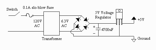
When building the circuit, all wiring should be kept as short as possible. This is especially true of the clocks for the AD1890 and CS8402, which should be mounted as close as possible to the chips. One simplification that can be done is substituting a 5V DC wall wart for the power supply shown in figure 2. This will simplify the circuit, and should not increase the cost. The only requirement is that it be able to output at least 300mA.
If you need to contact Crystal Semiconductor for any reason, their number is 512-445- 7222. The number for Analog Devices is 617-329-4700.
The oscillator for the CS8402A can have one of two values depending on which sampling rate you would like to output.
The 6.144MHz oscillator can be ordered from any crystal oscillator supplier such as Digi-Key (1-800-344-4539), part number SE1226-ND. The 5.6448MHz oscillator is a nonstandard value, and will have to be custom ordered. One place is JAN Crystals in Ft. Myers, Florida, part number JANXO-BACN5.6448. Their telephone number is 941-936-2397, and the cost is $13 plus shipping. The 16MHz oscillator for the AD1890 can also be ordered from Digi-Key, part number SE1211-ND.
Prices as of July 1996.
Allied Electronics has a $25.00 minimum. They carry the AD-1890, but it's $24.00. There are some components in the parts listed above with Allied Ellectronis parts numbers so that this minimum can be cleared.
I would like to thank Paul Stamler, Jeremy Moskowitz, Dan Vincent, and Scott Dorsey for their help in debugging the article.
All resistors 5% or less, 1/4 watt or more